
Electronic Packaging with Ceramic Substrates: Exploring Material Options
- Iva Leung
- Jan 17, 2024
- 2 min read

When it comes to the materials used in electronic packaging, ceramic substrates play a crucial role. These substrates come in various types, including HTCC, LTCC, TFC, DBC, and DPC, each offering distinct features and manufacturing processes.
Ceramic substrates, owing to their excellent thermal conductivity, heat resistance, electrical insulation, low thermal expansion coefficient, and cost-effectiveness, find increasing applications in electronic packaging. Particularly, they are extensively utilized in devices like IGBTs (Insulated Gate Bipolar Transistors), LDs (Laser Diodes), high-power LEDs (Light Emitting Diodes), and CPV (Concentrated Photovoltaics) packaging.
Key ceramic materials include alumina (Al2O3), aluminum oxide (Al2O3), aluminum nitride (AlN), and silicon nitride (Si3N4). Among these, Si3N4 ceramic substrates stand out for their superior electrical insulation, chemical stability, thermal stability, and mechanical strength, making them ideal for manufacturing large integrated circuit boards in high-integration applications.
Let's compare the performance of several ceramic materials:
High-Temperature Co-Fired Ceramic (HTCC):
Manufacturing involves blending ceramic powder (Al2O3 or AlN) with organic binders to form a paste.
The paste is shaped into sheets, dried to form green sheets, and then processed with hole drilling for layer-specific design.
Metal paste is screen-printed for wiring and filling, followed by sintering at high temperatures.
Limitations include high sintering temperatures, restricting the choice of metal conductors (e.g., tungsten, molybdenum, manganese), resulting in a moderate thermal conductivity of 20–200W/(m).
Low-Temperature Co-Fired Ceramic (LTCC):
Similar to HTCC, but with the addition of low-melting-point glass material to lower the sintering temperature (850–900°C).
Challenges include possible misalignment in network issues during screen-printing of metal lines and differential shrinkage during multi-layer ceramic stacking, affecting the yield.
To enhance thermal conductivity, additional cost may be incurred by introducing thermal and electrical via holes in the chip area.
Thick-Film Ceramic (TFC):
Unlike LTCC and HTCC, TFC is a post-ceramic substrate.
Metal paste is applied to the ceramic base surface using screen-printing technology, followed by drying and high-temperature sintering (700–800°C).
The resin is burned off during sintering, leaving almost pure metal due to the glassy bonding effect on the ceramic substrate surface.
With maturity, simplicity, and low cost, TFC finds applications in electronic packaging with lower graphic precision requirements.
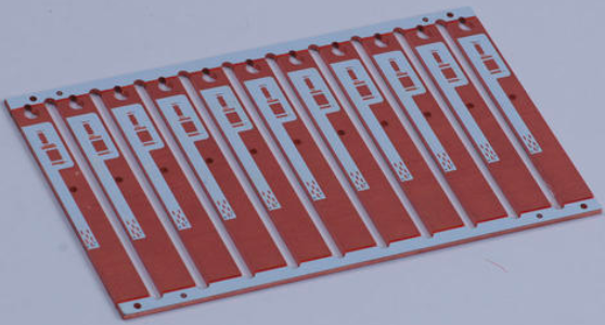
Direct Bonded Copper Ceramic Substrate (DBC):
Ceramic and copper foil are co-sintered at a high temperature (1065°C), forming a composite structure.
Copper foil is etched to create wiring based on design requirements.
DBC offers advantages such as good thermal conductivity, strong insulation, and high reliability, making it widely used in IGBTs, LDs, and CPV packaging.

DBC's drawbacks include the high control requirements for the eutectic reaction between Cu and Al2O3 at high temperatures. Additionally, the high-cost Al2O3 and the copper layer are prone to micro-holes, leading to decreased heat shock resistance. Hence, the thickness of copper foil on the DBC surface is generally above 100µm.


Comentarios